PCB Process Capability
| No. | Project | Technical indicators |
| 1 | Layer | 1-60(layer) |
| 2 | Maximum processing area | 545 x 622 mm |
| 3 | Minimumboardthickness | 4(layer)0.40mm |
| 6(layer) 0.60mm | ||
| 8(layer) 0.8mm | ||
| 10(layer)1.0mm | ||
| 4 | Minimum line width | 0.0762mm |
| 5 | Minimum spacing | 0.0762mm |
| 6 | Minimum mechanical aperture | 0.15mm |
| 7 | Hole wall copper thickness | 0.015mm |
| 8 | Metallized aperture tolerance | ±0.05mm |
| 9 | Non-metallized aperture tolerance | ±0.025mm |
| 10 | Hole tolerance | ±0.05mm |
| 11 | Dimensional tolerance | ±0.076mm |
| 12 | Minimum solder bridge | 0.08mm |
| 13 | Insulation resistance | 1E+12Ω(normal) |
| 14 | Plate thickness ratio | 1:10 |
| 15 | Thermal shock | 288 ℃(4 times in 10 seconds) |
| 16 | Distorted and bent | ≤0.7% |
| 17 | Anti-electricity strength | >1.3KV/mm |
| 18 | Anti-stripping strength | 1.4N/mm |
| 19 | Solder resist hardness | ≥6H |
| 20 | Flame retardancy | 94V-0 |
| 21 | Impedance control | ±5% |
We do Multi-layer HDI PCB Circuit Boards with 15 years' experience with our professionalism
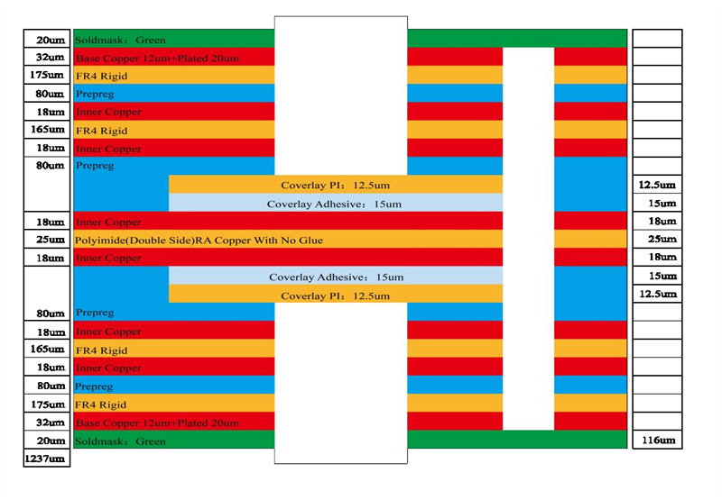
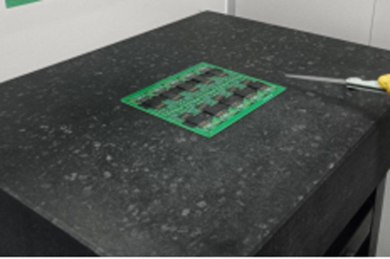
8 layer HDI Printed Circuit Boards
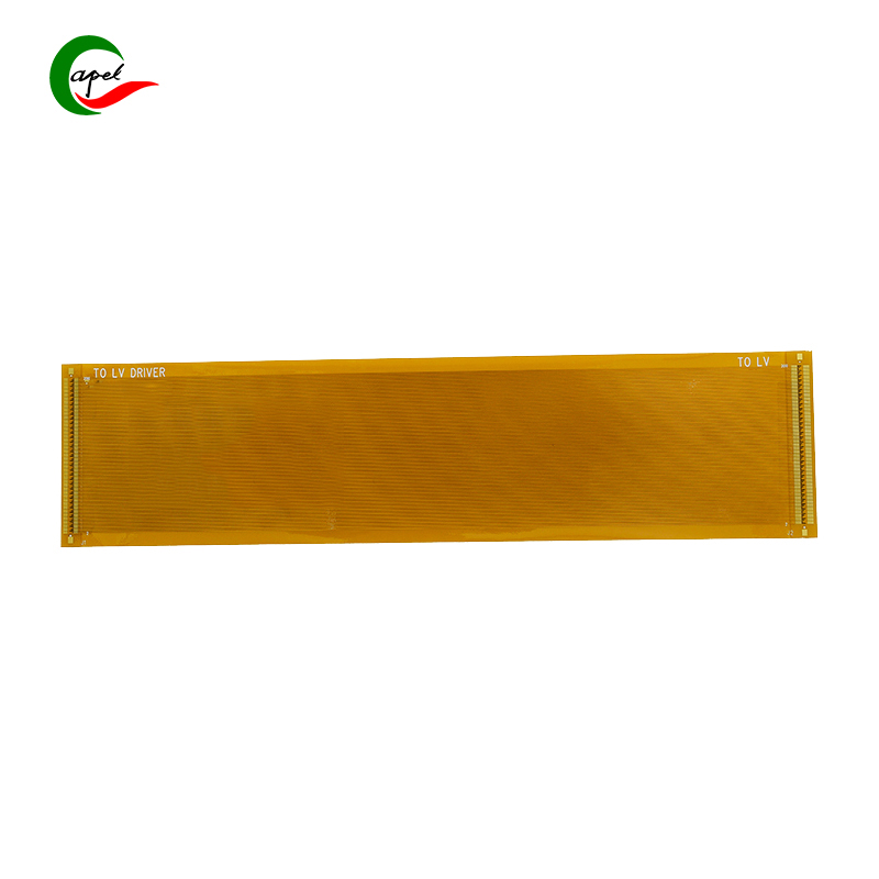
4 layer Flex-Rigid Boards
8 layer Rigid-Flex PCBs
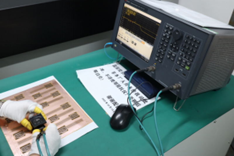
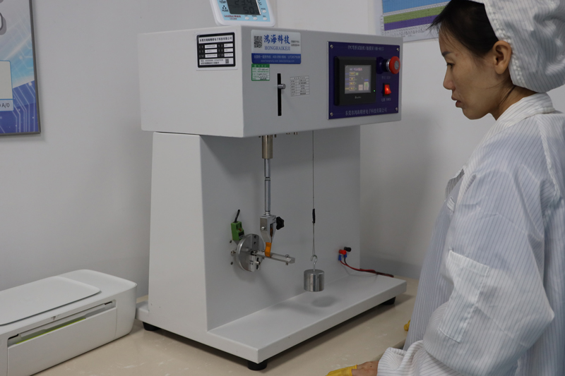
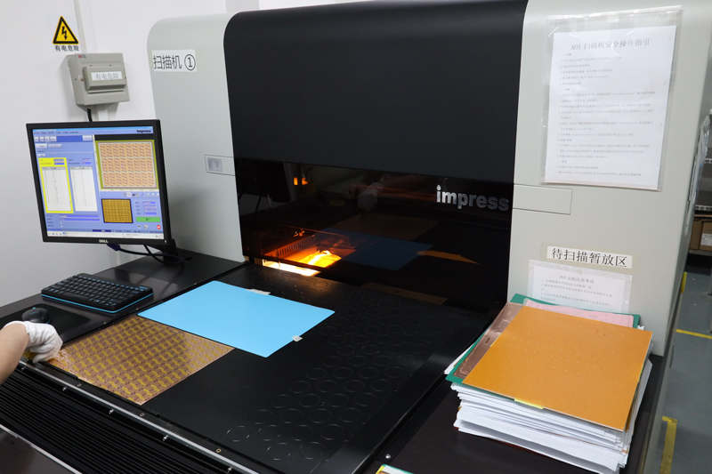
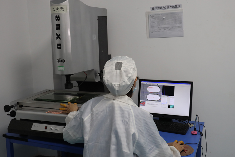
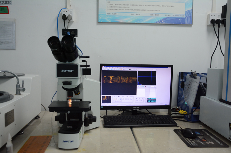
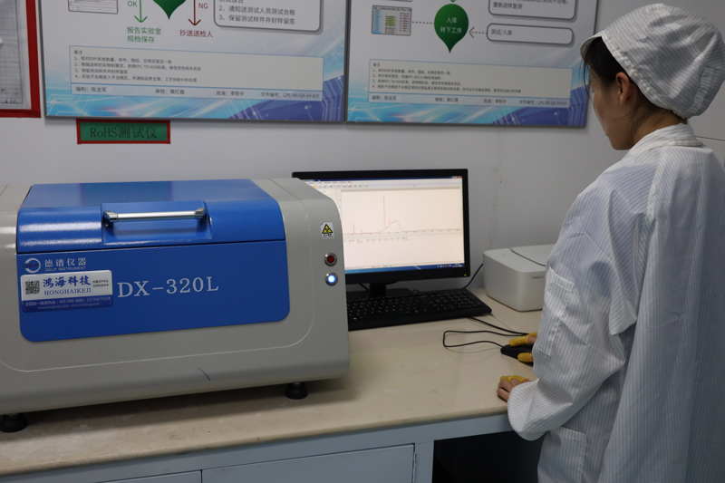
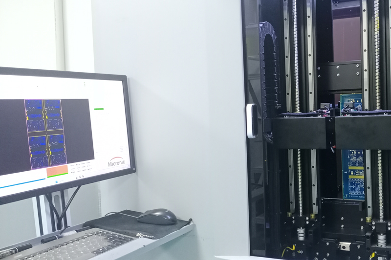
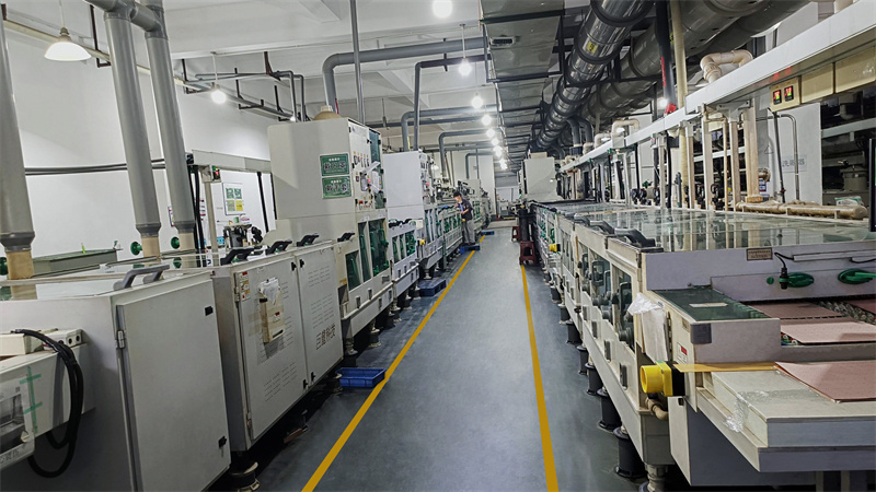
Testing and Inspection Equipment
What are the benefits of choosing an HDI board?
. Provide technical support Pre-sales and after-sales; . Custom up to 40 layers, 1-2days Quick turn reliable prototyping, Component procurement, SMT Assembly; . Caters to both Medical Device, Industrial Control, Automotive, Aviation, Consumer Electronics, IOT, UAV, Communications etc.. . Our teams of engineers and researchers are dedicated to fulfilling your requirements with precision and professionalism.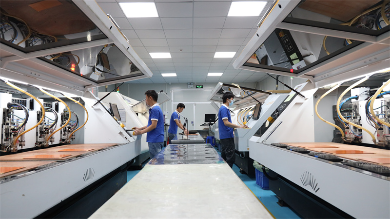
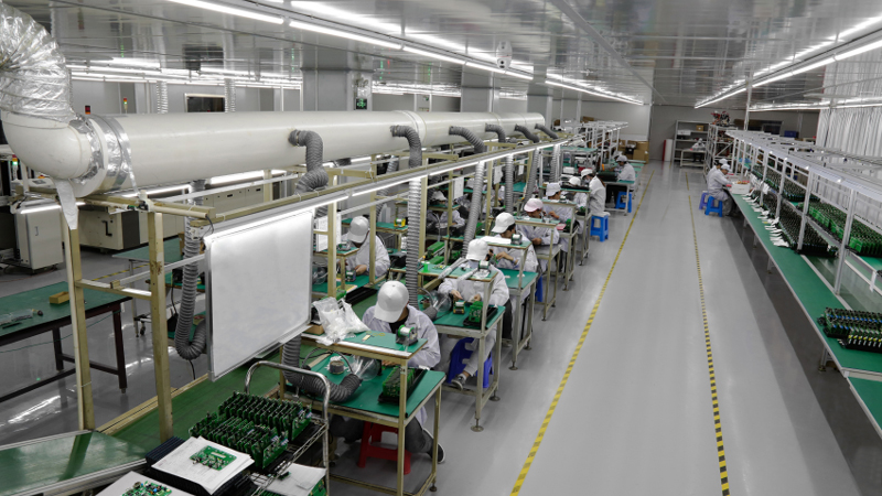
Our Multi-layer HDI PCB Circuit Boards Service
1. Improved thermal management: Compared with traditional PCBs, HDI PCBs can provide better thermal management. The compact layout and reduced number of layers increase the thermal efficiency of the components, resulting in lower operating temperatures. This is especially beneficial for electronics that generate a lot of heat, such as power electronics, LED lighting, and high-performance computers. 2. Cost-effective: Although HDI PCBs may initially seem more expensive due to their advanced technology, they are actually cost-effective in the long run. The smaller form factor allows more boards to be produced from a single panel, reducing unit production costs. Additionally, a compact layout can reduce material costs, as fewer raw materials are required. 3. Improved electrical performance: HDI PCB provides better electrical performance due to optimized wiring and shorter signal paths. This results in reduced signal loss, improved signal integrity and reduced power consumption. These factors are especially important for applications requiring high performance and energy efficiency. 4. Miniaturization: One of the main advantages of HDI PCBs is their ability to support miniaturization. HDI PCBs create smaller, lighter electronic devices by densely packing components and using smaller vias and traces. This is especially valuable in industries where size and weight constraints are critical, such as aerospace and consumer electronics. 5. Compatibility with advanced components: HDI PCB technology is ideal for integrating advanced components such as microprocessors, memory chips, sensors, and high-density connectors. The improved design flexibility and smaller size of HDI PCBs allows for the seamless integration of these components, enabling more advanced functions and features in electronic devices. 6. Faster time to market: HDI PCB can speed up the product development process and reduce time to market. The HDI PCB's compact design and improved signal integrity facilitate easier testing, debugging, and prototype iterations, reducing product development cycles. 7. Environmental benefits: HDI PCBs contribute to environmental sustainability by using less raw materials and reducing waste generation. The smaller size and reduced material requirements help conserve resources, minimize waste disposal, and promote environmentally friendly manufacturing practices. 8. Scalability: HDI PCB technology has scalability and the ability to adapt to changing industry needs. As technology advances and new electronic components become available, HDI PCBs can accommodate these changes, allowing for future upgrades and improvements without a complete redesign.
 HDI Circuit Board FAQ
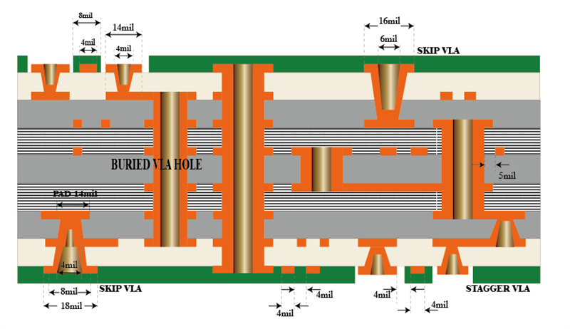
1. What is HDI circuit board? HDI stands for High Density Interconnect. An HDI board is a printed circuit board (PCB) that utilizes advanced design and manufacturing techniques to achieve higher circuit density and more functionality in a smaller form factor. 2. What are the advantages of HDI circuit boards? HDI boards offer several advantages, including: - Higher routing density: HDI boards allow for more complex and compact layouts, enabling more components to be placed on smaller boards. - Improved Signal Integrity: With shorter interconnects and lower noise, HDI boards provide enhanced signal quality and integrity, which is critical for high-speed and high-frequency applications. - Enhanced reliability: Advanced manufacturing techniques in HDI boards, such as microvias and fine-pitch traces and spaces, allow for increased reliability and better performance. - Miniaturization: HDI technology enables circuit boards to be developed smaller and thinner for various advanced electronic devices. - Cost optimization: While HDI boards may involve a more complex manufacturing process, they can often reduce overall system cost by eliminating the need for additional components and reducing overall board size.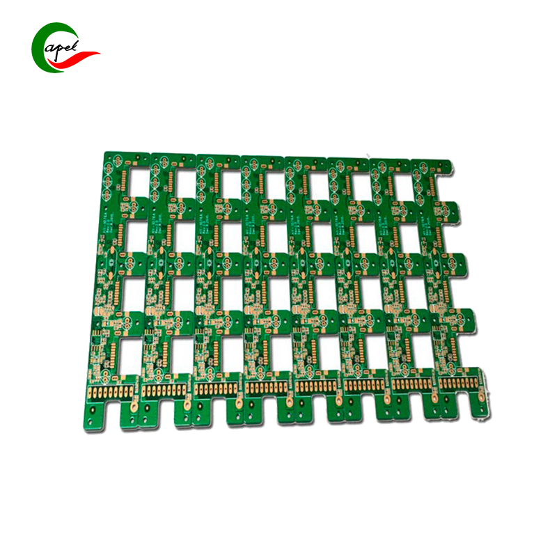 3. What are the different types of HDI boards? There are many types of HDI boards, including: - 1+N+1 HDI: Multilayer with microvias and buried vias, allowing high-density interconnects. - 2+N+2 HDI: Similar to 1+N+1, but with additional buried vias for added complexity. - Any layer HDI: All layers contain microvias, enabling high levels of interconnectivity and density. - Staggered Via HDI: Staggered vias stacked to achieve high density with a relatively simple design. 4. What applications are HDI boards generally used for? HDI circuit boards are widely used in various applications requiring compact size, high performance, and advanced functionality. Some common applications include: - Mobile Devices: Smartphones, tablets and wearables often rely on HDI boards for their compact size and high speed requirements. - Medical equipment: Medical equipment such as imaging systems, patient monitoring equipment, and diagnostic instruments benefit from HDI boards for their increased functionality and reliability. - Aerospace and Defense: HDI boards are ideal for aerospace and defense applications requiring advanced functionality in space-constrained environments. - Automotive Electronics: With the continuous advancement of automotive technology, HDI circuit boards are used in vehicles to implement advanced driver assistance systems (ADAS), infotainment systems, and other electronic components. - Industrial equipment: HDI boards are increasingly used in industrial equipment such as robots, automation systems, and control equipment to achieve smaller form factors and higher performance.