PCB Process Capability
| No. | Project | Technical indicators |
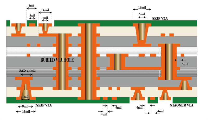
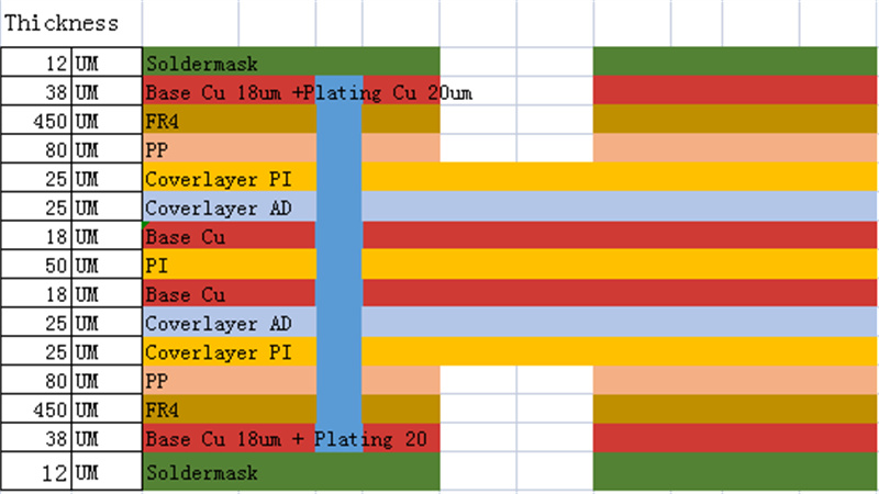
| 1 | Layer | 1-60(layer) |
| 2 | Maximum processing area | 545 x 622 mm |
| 3 | Minimumboardthickness | 4(layer)0.40mm |
| 6(layer) 0.60mm | ||
| 8(layer) 0.8mm | ||
| 10(layer)1.0mm | ||
| 4 | Minimum line width | 0.0762mm |
| 5 | Minimum spacing | 0.0762mm |
| 6 | Minimum mechanical aperture | 0.15mm |
| 7 | Hole wall copper thickness | 0.015mm |
| 8 | Metallized aperture tolerance | ±0.05mm |
| 9 | Non-metallized aperture tolerance | ±0.025mm |
| 10 | Hole tolerance | ±0.05mm |
| 11 | Dimensional tolerance | ±0.076mm |
| 12 | Minimum solder bridge | 0.08mm |
| 13 | Insulation resistance | 1E+12Ω(normal) |
| 14 | Plate thickness ratio | 1:10 |
| 15 | Thermal shock | 288 ℃(4 times in 10 seconds) |
| 16 | Distorted and bent | ≤0.7% |
| 17 | Anti-electricity strength | >1.3KV/mm |
| 18 | Anti-stripping strength | 1.4N/mm |
| 19 | Solder resist hardness | ≥6H |
| 20 | Flame retardancy | 94V-0 |
| 21 | Impedance control | ±5% |
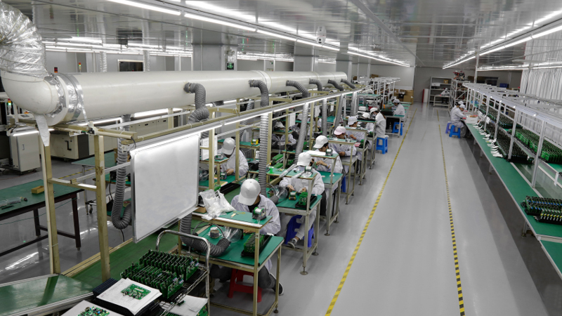
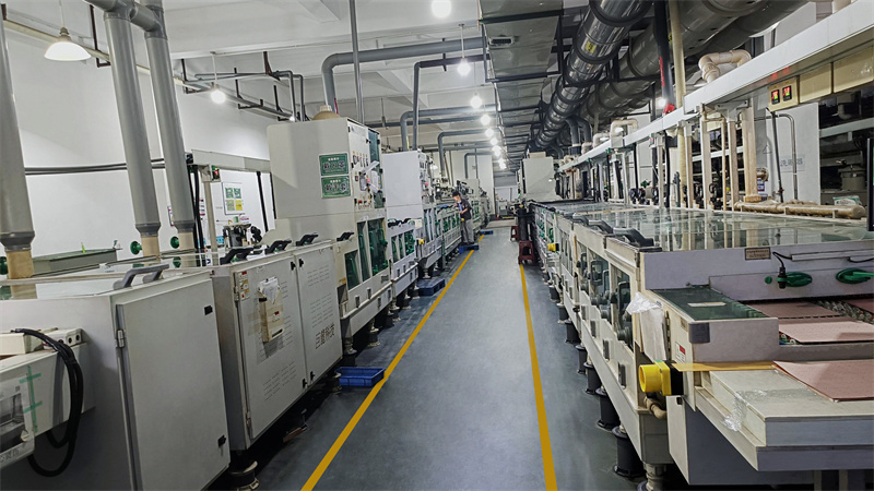
We do Circuit Boards Prototyping with 15 years' experience with our professionalism
8 layer HDI Printed Circuit Boards
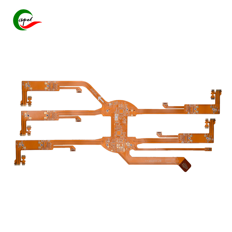
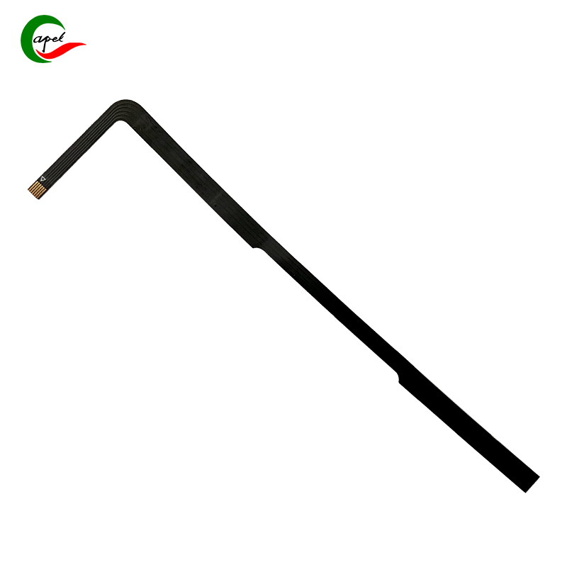
4 layer Flex-Rigid Boards
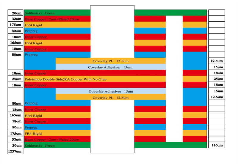
8 layer Rigid-Flex PCBs
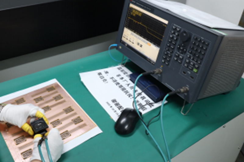
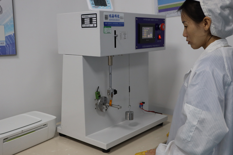
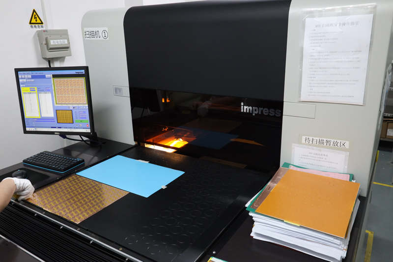
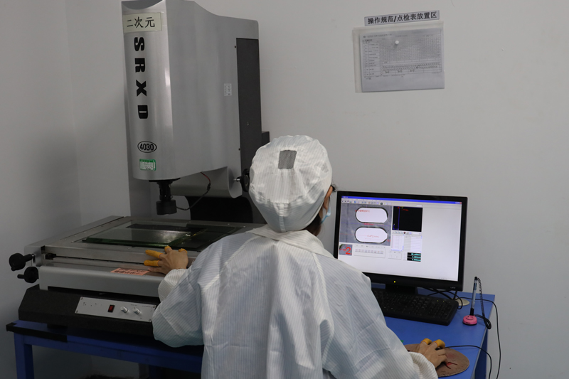
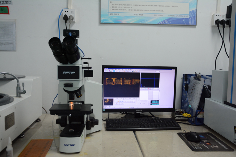
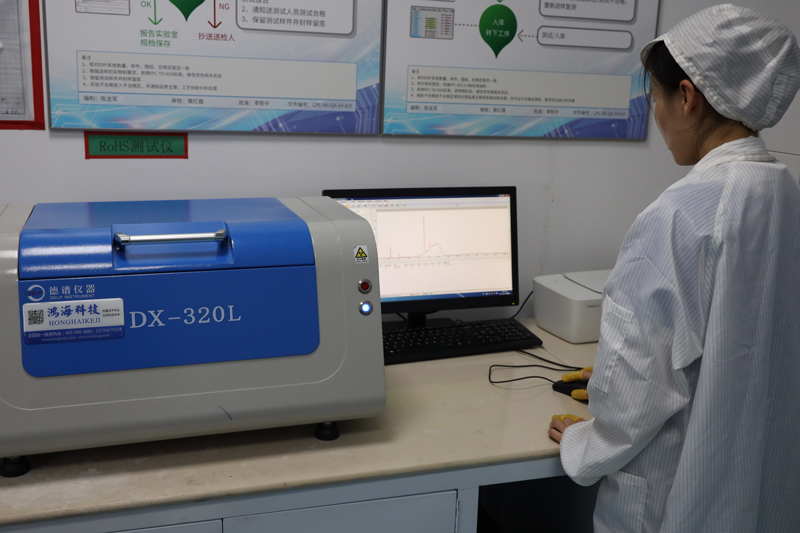
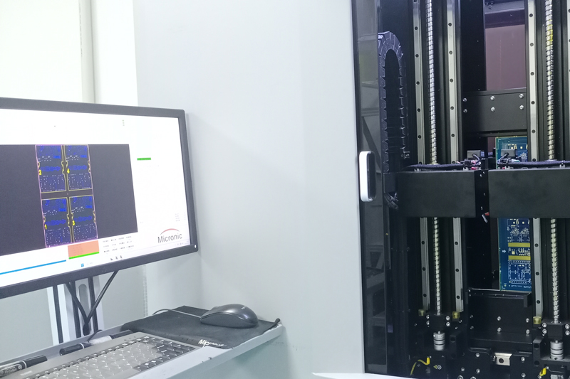
Testing and Inspection Equipment
How to manufacture a high- quality Double-Sided Circuit Boards?
. Provide technical support Pre-sales and after-sales; . Custom up to 40 layers, 1-2days Quick turn reliable prototyping, Component procurement, SMT Assembly; . Caters to both Medical Device, Industrial Control, Automotive, Aviation, Consumer Electronics, IOT, UAV, Communications etc.. . Our teams of engineers and researchers are dedicated to fulfilling your requirements with precision and professionalism.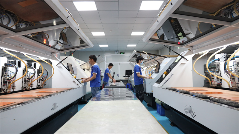
Our Circuit Boards Prototyping Service
1. Design the board: Use computer-aided design (CAD) software to create the board layout. Ensure that the design meets all electrical and mechanical requirements, including trace width, spacing, and component placement. Consider factors such as signal integrity, power distribution, and thermal management. 2. Prototyping and testing: Before mass production, it is critical to create a prototype board to validate the design and manufacturing process. Thoroughly test prototypes for functionality, electrical performance, and mechanical compatibility to identify any potential issues or improvements. 3. Material Selection: Choose a high-quality material that suits your specific board requirements. Common material choices include FR-4 or high-temperature FR-4 for the substrate, copper for conductive traces, and solder mask to protect components.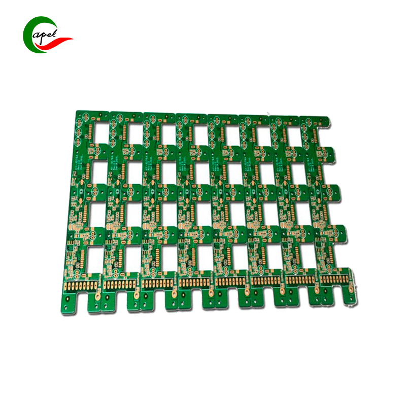 4. Fabricate the inner layer: First prepare the inner layer of the board, which involves several steps: a. Clean and roughen the copper clad laminate. b. Apply a thin photosensitive dry film to the copper surface. c. The film is exposed to ultraviolet (UV) light through a photographic tool containing the desired circuit pattern. d. The film is developed to remove the unexposed areas, leaving the circuit pattern. e. Etch exposed copper to remove excess material leaving only desired traces and pads. F. Inspect the inner layer for any defects or deviations from design. 5. Laminates: Inner layers are assembled with prepreg in a press. Heat and pressure are applied to bond the layers and form a strong panel. Make sure the inner layers are properly aligned and registered to prevent any misalignment. 6. Drilling: Use a precision drilling machine to drill holes for component mounting and interconnection. Different sizes of drill bits are used according to specific requirements. Ensure the accuracy of hole location and diameter.
 How to manufacture a high- quality Double-Sided Circuit Boards?
7. Electroless Copper Plating: Apply a thin layer of copper to all exposed interior surfaces. This step ensures proper conductivity and facilitates the plating process in subsequent steps. 8. Outer layer imaging: Similar to the inner layer process, a photosensitive dry film is coated on the outer copper layer. Expose it to UV light through the top photo tool and develop the film to reveal the circuit pattern. 9. Outer layer etching: Etch away the unnecessary copper on the outer layer, leaving the required traces and pads. Check the outer layer for any defects or deviations. 10. Solder Mask and Legend Printing: Apply solder mask material to protect copper traces and pads while leaving area for component mounting. Print legends and markers on top and bottom layers to indicate component location, polarity, and other information. 11. Surface Preparation: Surface preparation is applied to protect the exposed copper surface from oxidation and to provide a solderable surface. Options include hot air leveling (HASL), electroless nickel immersion gold (ENIG), or other advanced finishes.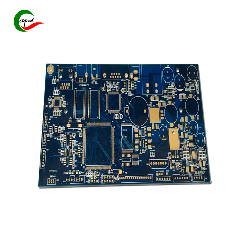 12. Routing and Forming: PCB panels are cut into individual boards using a routing machine or V-scribing process. Make sure the edges are clean and the dimensions are correct. 13. Electrical Testing: Perform electrical testing such as continuity testing, resistance measurements, and isolation checks to ensure the functionality and integrity of the fabricated boards. 14. Quality Control and Inspection: Finished boards are thoroughly inspected for any manufacturing defects such as shorts, opens, misalignments, or surface defects. Implement quality control processes to ensure compliance with codes and standards. 15. Packing and Shipping: After the board passes the quality inspection, it is packed securely to prevent damage during shipping. Ensure proper labeling and documentation to accurately track and identify boards.